Abstract
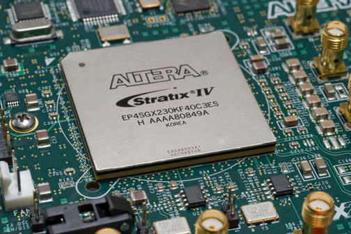
Before the widespread adoption of Field-Programmable Gate Arrays (FPGAs), the most common tools for optimising complex electrical systems were ASICs (Application-Specific Integrated Circuits) and PLDs (Programmable Logic Devices). Although seminal to the development of the Electronic Engineering field, their steep and costly downsides made the creation of the FPGA necessary. FPGAs emerged as a technology that was essentially an infinitely reprogrammable cluster of arbitrary gates that could be rearranged to emulate various complexities of electrical systems. This brief literature review explores the key architectures that define modern-day FPGAs.
Technology
Early PALs and PLDs used permanent fuse technology to create the desired pathways in the device, while modern FPGAs employ different types of programming technologies to ensure that the hardware can be used more than once.
SRAM cell architecture is most commonly used in modern FPGAs. An FPGA can be made up of millions of SRAM cells put next to each other, and they can either store a value of 1 or 0, as is assigned to them by the uploaded program. The main drawback of this architecture is the amount of area that it uses, with 6 MOSFETs needed to activate a single cell. This is coupled with the fact that the memory in these cells is volatile, which creates the need for external memory such as EPROMs. Conversely, this technology is infinitely reprogrammable, which is a huge financial and tactical advantage to all of the engineers using it, and was the main setback of its PLD predecessors.
Antifuse architecture is similar to that of the early ASICs in the fact that they are non-reversible after they are programmed for the first time. Small wires are crossed over each other and are separated by a layer of amorphous silicon, which is non-conductive due to a high level of resistance. When a high voltage is applied to the link, it overcomes the resistance and allows more current to flow through. Due to the nature of the connections, an antifuse FPGA is smaller, but has the obvious limitation of being permanent. However, in systems where the chip is required to operate in suboptimal conditions (e.g., radiation), antifuse FPGAs are more widely implemented, as the connections are less affected by the environment [2].
Unlike the other two architectures, the base state for floating-gate FPGAs is 1. All the cells, which are made up of floating gates that start as "open switches", can be written to have a state of 0, which disconnects the route. It can be reconfigured thousands of times using the same electronic "wiping" system as early EEPROMs, but repeated wiping can cause the connections to wear out. The main drawback of this architecture is that it has a high switch resistance, which dissipates more power. This is balanced by the fact that its memory is non-volatile and it has an instant boot time.
Logic-Block Granularity
The infinite reconfigurability of FPGAs is what makes it such a powerful tool, and this property is made possible by the flexibility of its Logic-Block architecture. Fundamentally, everything electronic is made of transistors, and by extension, gate logic; implementing clusters of the aforementioned cells into Logic Blocks allows FPGAs to emulate arbitrary gates.
For SRAM-based architecture, the main logic method is LUTs (Look-Up Tables), which are simply configurable truth tables. Varying numbers of SRAM cells make up a LUT (dependent on the coarseness), and when a program is uploaded to the FPGA, the LUT can assume the identity of any truth table from any gate arrangement. This, however, depends on the LUT's granularity. A fine-grained LUT can only emulate the output of a two-input logic gate arrangement, such as an AND, OR, or an XOR gate, but it takes up less physical space. Coarse-grained LUTs can emulate up to six-input arrangements but take up more space. Specifically, in order to implement a 6-input table, 64 cells are needed, which increases the used silicon area significantly. As the coarseness of the LUTs increases, their density decreases, as fewer of them need to be used; however, the area used increases, as coarser LUTs require more physical circuitry. This logic architecture is the most frequently used in modern FPGAs, but there is also a separate, more dated architecture called multiplexer logic that has been phased out over the years due to its inefficiency.
Routing Architectures
To optimise the power consumption, the arrangement of the wires connecting the individual connection blocks must be carefully planned. The routing of logic blocks is mostly done through individual wires that either lie vertically or horizontally, and at the intersections of these wires, there are switch blocks which connect the perpendicular wires so that logic blocks can "communicate" with each other. Each of these wires is a specific type of wire, and most FPGAs have four essential types. General purpose: the wires that connect to and through switch blocks; Direct (short) wire: the wires that connect exclusively to their surrounding logic blocks and nothing else; Long wire: the wires that connect more distant parts in a direct connection; and finally a global clock line that synchronises all actions in the chip. Different manufacturers choose to route their chips differently, but the struggle is to minimize the number of stops the signal has to make (i.e. at a switch block) and delay (caused by long wire), while also maximising the signal speed and leftover surface area.
References
- J. Rose, A. El Gamal and A. Sangiovanni-Vincentelli, "Architecture of field-programmable gate arrays," in Proceedings of the IEEE, vol. 81, no. 7, pp. 1013-1029, July 1993, doi: 10.1109/5.231340.
- V. M. Placinta, L. N. Cojocariu, F. Maciuc and M. Straticiuc, "Single Event Effects and Total Ionizing Dose Sensitivity of a 0.15 μm Antifuse FPGA," 2023 IEEE Nuclear Science Symposium, Medical Imaging Conference and International Symposium on Room-Temperature Semiconductor Detectors (NSS MIC RTSD), Vancouver, BC, Canada, 2023, pp. 1-1, doi: 10.1109/NSSMICRTSD49126.2023.10337877.
- P. Y. K. Cheung, "Tutorial on FPGA: Architecture of Field Programmable Gate Arrays," Department of Electrical and Electronic Engineering, Imperial College London, Course Lecture Notes. Available: ee.ic.ac.uk